You should be diff'ing your PCBs before going to production.
Software engineering has used visual diff tools for production workflows since the 1990s. It's 2026 and hardware engineers still ship production PCBs to fab without this critical verification step. The average PCB respin in production is estimated to cost $28,000. Engineers make mistakes, but it's the release process that fails to catch those errors that is truly to blame.
The change you didn't see
Here's the scenario: A junior EE at your company creates a new SOIC-8 footprint for a prototype with a subtle pinout error and unintentionally overwrites it into the production component library. Later, you (a senior EE) update a different design already in production. You rebuild the Gerbers for a minor silkscreen update. The library change comes along for the ride. You have no reason to look at that footprint; it isn't what you changed. The board goes out for fabrication, and when your PCBAs show up dead on arrival, your end assembly production is down until you can cut a new PCB revision or manually white-wire every PCB by hand.
This nightmare happens at every company, big and small. It's easy to blame the individual engineer. The junior should have known not to touch the production component library. You should have caught the footprint change. But the reality is that the release process is fundamentally flawed, there are no checks on the actual files going to fab.
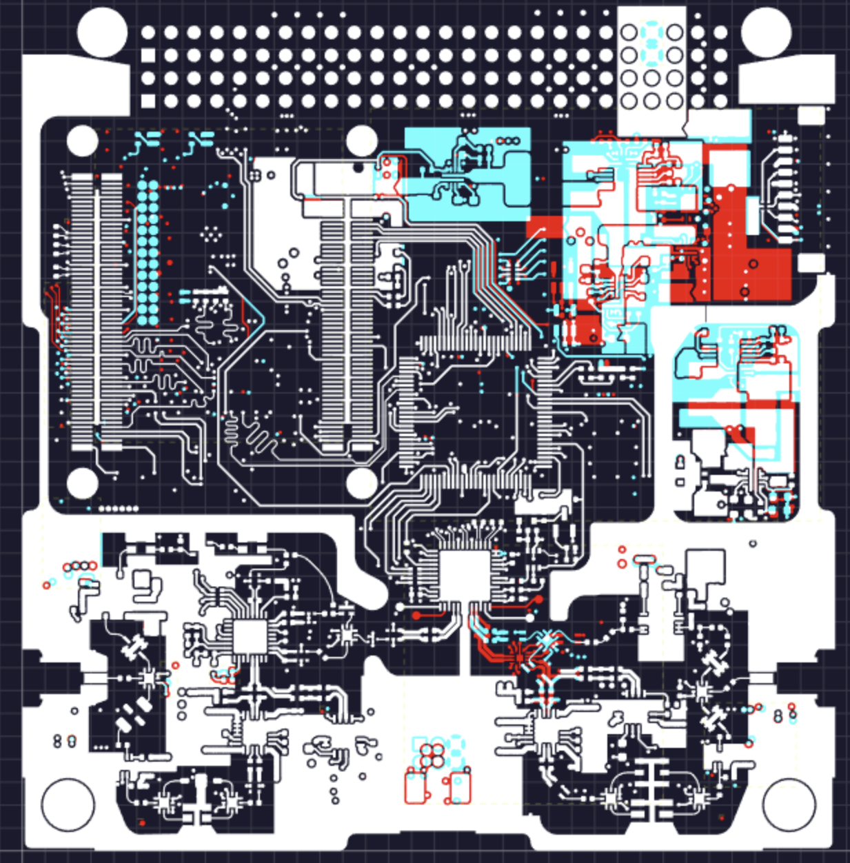
An unexpected footprint change is just one hypothetical scenario. The pad that lost its thermal relief. The drill file that's missing because someone forgot to include NPTH on the gerber output. The inner polygon pour that became an island because of a rule change. The connector pinout that mirrored during a library migration. None of these errors are hard to see if you look. But Gerber files are not designed for human review.
A typical 4-layer production board generates thousands of coordinate commands and aperture definitions across its layers, and even experienced engineers miss subtle differences when eyeballing two nearly identical layouts. Manual Gerber comparison is impractical for production review[1]. The schematic doesn't catch it. The PDF print doesn't catch it. The DRC doesn't catch it. An independent visual diff does.
What a missed revision costs
The numbers are public, and they're not small. From an I-Connect007 design article on DRC and respin economics:
EMA Design Automation breaks the same number out for complex high-speed work and gets a wider range:
Their worked example for a PCIe Gen5 board: $12,000 hard costs (fab, assembly, parts), $24,000 engineering labor (rework, retest), and $50,000 of opportunity cost: the schedule slip from a missed launch window. That last number is usually the one the engineering manager actually feels.
And it's not one respin. An Aberdeen study cited in industry literature found that non-integrated PCB design flows average 14.1 physical prototypes for a moderately complex board, with prototypes accounting for 31% of total product cost. Even mature workflows still average around 3 spins to production.
One avoided respin pays for years of an individual GerbDiff subscription. This is the kind of math where the ROI calculation isn't a calculation: the tool is a necessity in a production environment.
The diff tool shouldn't be the EDA tool
Trust but verify. You wouldn't accept a security audit from the same company that wrote the code, or a financial audit from the company's own CFO. PCB review is the same: the tool that generated the Gerbers is the worst possible tool to check them.
Here's the practical version of the same argument: the fab house that builds your board doesn't use Altium, KiCad, OrCAD, or whatever EDA generated your files. They use CAM tools that read the Gerbers as bytes, exactly as the photoplotter will. If you're not also reading those bytes through a tool that's independent of your EDA, you and your fab are looking at two different designs.
Every EDA tool also has its own Gerber creation/parsing quirks: aperture macro expansion edge cases, polygon-pour changes between versions, silent plot-scaling differences. The tool that produced the artifact is structurally unable to detect its own bug. It shows you the design as it intended to render, not as the fab will receive it. A third-party diff tool sees what the photoplotter sees.
How teams handle PCB revisions today (and where each breaks)
Walk into ten hardware shops on the way to a production tapeout and you'll see roughly three workflows. They share a common failure mode: none of them put an independent set of eyes between the Gerbers and the fab.
1. Eyeball the two designs in the source EDA
The designer or reviewer opens both revisions in Altium, KiCad, or Eagle and visually compares. Breaks three ways at once: confirmation bias (whoever's looking already "knows" what it should look like), the EDA renders both revisions with the same internal model (including any rendering quirks), and you're scanning manually with no layer pairing or change clustering. You're not seeing what the fab will see; you're seeing what the EDA thinks the design is.
2. Trust the EDA's built-in "what changed" report
Most EDAs have a version-compare feature that diffs the design database: the schematic, the layout, the source-of-truth project files. Breaks because the design database isn't what gets fabricated. The Gerber files emitted at plot time are. And those drift from the design database in ways the EDA's compare can't see: CAM operators hand-edit Gerbers between plot and tapeout, the fab adds panelization on top of what you sent (rails, fiducials, tooling holes), plot settings change across team members, and library updates silently shift component geometry between plots. You have to compare the exact bytes going to the fab, not the EDA's internal model of what they should look like.
3. Skip the review entirely and rely on the fab house
"The fab will catch it; they run DFM." Breaks because fab DFM checks manufacturability (can this be built), not design intent (does this match what you wanted). The fab doesn't have your previous revision to compare against. The fab doesn't know which 5-mil delta matters. And the fab is incentivized to build whatever you send. They get paid either way.
The shared failure mode is independence. The review and the design come from the same source: the designer reviews their own work, the EDA reviews its own output, or the fab (which has no design context) is asked to catch problems it isn't equipped to catch. None of these workflows produce a record either, a thing you can attach to an Engineering Change Notice, link in a pull request, or pull up in a post-mortem. The review either happened in someone's head or didn't happen at all.
The Solution: GerbDiff
I built GerbDiff because I am an engineer who personally experienced the pain of not catching mistakes before PCBs went to production. GerbDiff has been built from the ground up to explicitly solve this problem. To highlight a few core features:
- From scratch Gerber parser → A Gerber parser built from scratch directly from UCAMCO design specifications. Validated against hundreds of real production jobs from KiCad, Altium, Eagle, OrCAD, and EasyEDA. It reads the bytes the photoplotter will read, not the in-memory model of the tool that produced them.
- Local processing → Always. Files never leave your machine. No telemetry of design content. Defense-grade by construction, not by promise.
- Difference Reports → PNG screenshots and self-contained HTML reports. Drop one into the ECN, the PR, the ticket, the post-mortem.
- Automatic layer pairing → Auto-detects layer roles across project revisions, even when file names changed or the project moved between EDA tools.
- Side-by-side and overlay → Both views, synchronized pan and zoom. Switch between them with a keystroke.
- GitHub Action → A free Action that automatically generates a layer-by-layer diff into every pull request that touches a board file. The same review surface your firmware team already uses. Now for the boards, too.
Back to your scenario
The junior still overwrote the library. You still rebuilt for that silkscreen update. The library change still came along for the ride. The difference: GerbDiff is in your release process, so you see the footprint change on the diff report and flag it before the design goes out. The production line stays up. Nobody stays late soldering white wires. Engineers made mistakes, and the process caught them. The way the process should.
Catch the next one before fab
30-day free trial. No credit card.
From $9/month or $99/year. One avoided respin pays for it for decades.
Sources
- PCBSync, How to Compare Two Gerber Files for Differences.
- I-Connect007 / Design007 Magazine, Design Rule Checks Cut Down Board Respins. The $28K figure is cited as an industry average.
- EMA Design Automation, The Cost of PCB Design Spins. Breakdown: ~20% hard cost, ~30% engineering labor, ~10% lab/test, ~40% opportunity cost.
- Aberdeen Group, Why Printed Circuit Board Design Matters to the Executive. Cited figure: 14.1 average physical prototypes in non-integrated design flows.
- Altium, Your PCB Design Review Process Is Obsolete. Background on how reviews actually happen on most hardware teams today.